Scanning electron microscopy - SEM
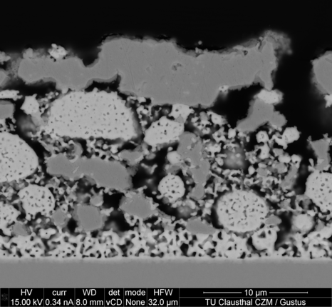
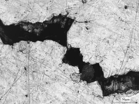
In scanning electron microscopy (SEM), a finely focused electron beam (a few nm) is moved across the surface in a raster and the secondary electron emission caused by interaction with the surface is measured at the same time. Scanning electron microscopy can be used to produce high-resolution images of surfaces with a high depth of field. Depending on the type of secondary electrons detected, SEM images can be taken with the usual topography contrast or with an additional material contrast. In addition to the topography, the latter also provides information about the element distribution on the surface. Today, scanning electron microscopy is one of the standard methods in material analysis. It forms the basis of numerous other methods, such as transmission electron microscopy (STEM), electron backscatter diffraction (EBSD) or energy-dispersive X-ray analysis (EDX).
Equipment: Helios Nanolab 600, Omicron NanoSAM
Scanning transmission electron microscopy - STEM
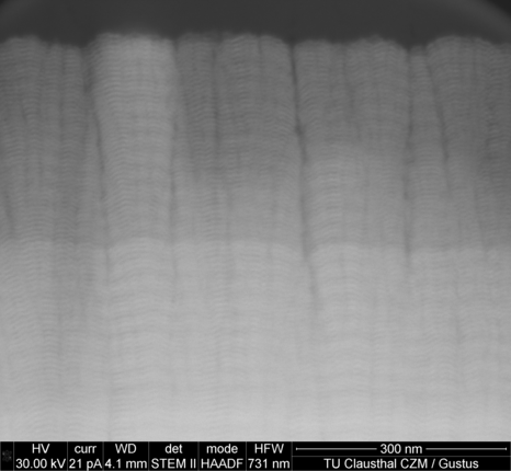
Scanning transmission electron microscopy (STEM) is an imaging technique that can be used to image the microstructure inside an object. Similar to scanning electron microscopy, a finely focused electron beam is scanned point by point over the object to be examined, in which case the electrons transmitted through the sample are detected and used to generate images. STEM can be used to measure samples up to a thickness of around 200 nm. For this purpose, the samples must be prepared on a corresponding TEM grid. In combination with the FIB technique, lamellae cut out of a material surface can also be analyzed using STEM.
Equipment: Helios Nanolab 600
Atomic force microscopy - AFM
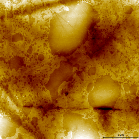
With the help of atomic force microscopy (AFM), the surface topography of a sample can be imaged and quantitatively analyzed. For this purpose, a so-called cantilever with a fine tip at its end is moved over the surface and the repulsive forces between the outer atoms of the tip and the surface are used as a control variable. Either the level of the repulsive force (z-position of the cantilever is kept constant) or the required readjustment of the tip-surface distance (repulsive force is kept constant) is used as the measured variable. In contrast to scanning electron microscopy, atomic force microscopy provides real height information in addition to the 2-dimensional representation of the topography. For example, the method is suitable for determining layer thicknesses or for measuring structured surfaces. Statistical parameters such as roughness values of a surface can also be determined.
Devices: Dimension DI-3100
Electron backscatter diffraction - EBSD
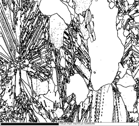
Electron backscatter diffraction (EBSD) is a crystallographic measurement method that can be used to obtain information about the crystal structure on the material surface. The EBSD technique is usually used in a scanning electron microscope and is based on the diffraction of elastically backscattered electrons at the crystal lattice surfaces of the solid. For the measurement, the sample is clamped at an angle of 70° to the primary electron beam and bombarded with electrons of defined energy. If the Bragg condition is fulfilled for incident electrons, constructive interference can occur. The measurement of the resulting diffraction pattern provides information about the crystal symmetry and crystal orientation. EBSD can also be used to obtain information about grain boundaries and stresses in the crystal structure. By coupling the measurement method with scanning electron microscopy, a spatially resolved analysis of the described crystal properties is possible.
Equipment: Helios Nanolab 600
Confocal laser microscopy - CLSM
In confocal laser microscopy (CLSM), the topography of the surface is recorded using laser beams. To do this, the laser is focused on the surface and the reflected light is measured behind a pinhole diaphragm. This technique enables lateral resolution to be improved by a third compared to a classic wide-field microscope. The sample is scanned plane by plane with the focus of the laser, whereby the height of a point on the surface can be quantitatively recorded in a similar way to atomic force microscopy. Confocal laser microscopy therefore enables the three-dimensional topographical imaging of a surface.
Devices: Keyence VK-X210
Nano-computed tomography - Nano-CT
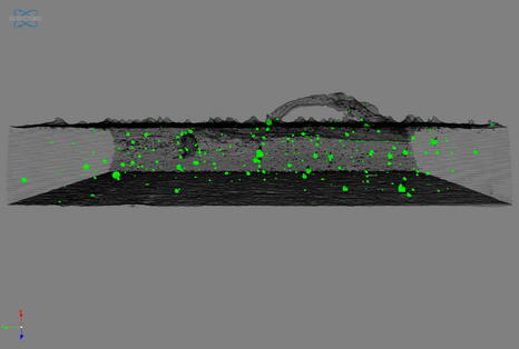
Computed tomography can be used to image the internal structure of an object non-destructively. For this purpose, the sample is irradiated with X-rays from different angles and the resulting shadow images are recorded. Computer-aided evaluation is used to reconstruct the 3-dimensional structure of the object. Computed tomography can be used, for example, to visualize pores, inclusions or defects inside a material.
Devices: Skyscan 2011
